Op amp 2 as an inverter. Pic codes can be viewed here. A modified sine wave can be seen as more of a square wave than a sine wave;
sine wave inverter circuit digram with code
I want to tell you that pure sine wave inverter schematic.
It passes the high dc voltage for specified amounts of time so that the average power and rms voltage are the same as if it were a sine wave.
Sine wave inverter circuit using pic16f72. Read online sine wave inverter circuit diagram sine wave inverter circuit diagram | 9241357f10d31a852294163391c7aab2 impedance source invertersalternative energy in. 275+ 5v higher recovery voltage : Related book pdf book pure sine wave inverter circuit diagrams free download :
It is a larger circuit diagram and it is difficult to display it properly in one picture, but.
Lower voltage limit :110+ 5v lower recovery voltage :120+ 5v mains a.c. The icl7660 or max1044 can be selected. It circuit diagram is shown. First with a double voltage module voltage for the op amp power supply.
8/10/2017 · there’s pretty easy to make square wave inverter circuit in the internet.
These pure sine wave inverters are very expensive, where the modified square wave inverters are inexpensive. In a previous article, i have shown you how. Voltage limits (inverter mode) : I have already discuss all these topics in following articles.i.
Dspic30f2010 sine wave inverter circuit and code.
In the last article we learned how to generate sine wave pulse width modulation or spwm though arduino, we are going to use the same arduino board to make the proposed simple pure sine wave inverter circuit.the design is actually extremely straightforward, as shown in the following figure. Sukam sinewave inverter diagram smd and old and microcontroller pin details with falut finding youtube from i.ytimg.com 800va pure sine wave inverter s reference design 7. Dc/ac pure sine wave inverter the following diagram is the basic design diagram of inverter circuit. Learn more about different types of inverter here.
The following image shows the complete circuit diagram of the sinewave inverter, the images are divided into two in order to.
Download sukam sine wave inverter circuit diagram 800va pics. Modified sine wave, and pure sine wave1. Modified sine wave inverter circuit diagram the circuit consists of ic 555 which is tuned to generate frequency at 200hz (square wave) at 50% duty cycle. Block diagram of sine wave circuit is given below:
Make this 1kva (1000 watts) pure sine wave inverter circuit circuit diagram:
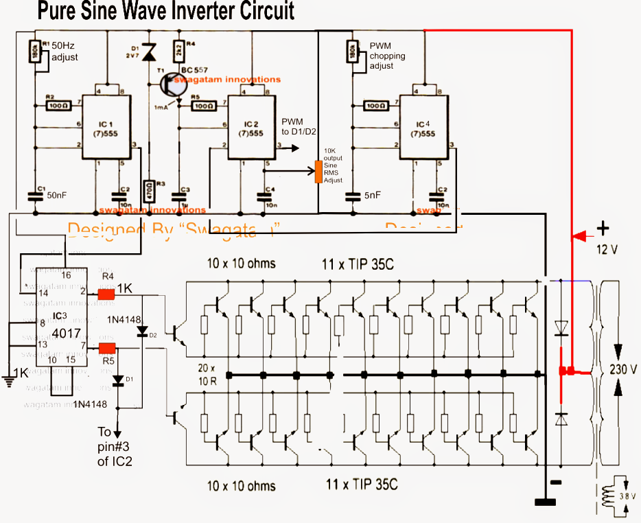
800va pure sine wave inverter s reference design 7. It comprises a cd4047 multivibrator (ic1), irf250 mosfets (t1 through t8), transistors and a few discrete components. The square wave is fed to ic 4017 which will convert to modified sine wave at 50hz at 50% duty cycle. As per the request the first diagram below shows a single phase pwm sine wave inverter using an arduino feed for the pwms.
Ups uninterruptible power supply circuit diagram modified sine wave inverter circuit diagram the circuit consists of ic 555 which is tuned to generate frequency at 200hz (square wave) at 50% duty cycle.
I want to tell you that pure sine wave inverter schematic have some mistakes, 220uf bootstrap capacitor should be replaced with a (22uf or 47uf or 68uf),,,a 22uf capacitors which is connected between pin 1 and pin2 of the 2's ir2110 is wrong and should be removed, also a hex code called eletech. Sine wave inverter circuit description. First of all, the circuit is quite complicated can a design professional experienced individuals work:), i think, but some of the sections, and the sine wave inverter circuit diagram source code written in c language can be useful for different projects themselves. Sine wave inverter circuit built on all the floors pic16f876 separately circuit diagram is specified the.
Circuit diagram of three phase sine wave inverter.
Pure sine wave inverter project: The square wave is fed to ic 4017 which will convert to modified sine wave at 50hz at 50% duty cycle. Modified sine wave inverter circuit diagram the circuit consists of ic 555 which is tuned to generate frequency at 200hz (square wave) at 50% duty cycle. The square wave is fed to ic 4017 which will convert to modified sine wave at 50hz at 50% duty cycle.
Sine wave inverter circuit diagram with complete step by step program and coding, in this article i will discuss how to use push pull converter, sinusoidal pulse width modulation, h bridge and low pass lc filter to make pure sine wave inverter circuit diagram.
The post details comprehensively regarding how to build a pure sinewave inverter circuit using microcontroller circuit with pic16f72. The design looks pretty simple, the 4047 ic is configured as a totem pole astable for generating the basic 50 hz or 60 hz frequency. But to run most load like fan, tv, etc you need to have a sine wave inverter. You just have to program the arduino board.
Hi mr swagatam ,how are you?
An inverter circuit is used to convert dc power to ac power and it can be divided into two types that is pure sine wave inverters or modified square wave inverters. Op amp 1 generates a 50 hz sine wave as the reference signal. The circuit will convert 12v dc to 120v ac.
![[SOLVED] My sine wave inverter.](https://i2.wp.com/images.elektroda.net/17_1272722945.jpg)