Circuit diagram of h bridge using ir2110. A unified approach for the control of power electronics converters. [5 marks] (iii) derive an expression.
Single phase Hbridge inverter. Download Scientific Diagram
[3 marks] (ii) assuming “a” is the angle of zero voltage at each side of the output voltage within a half cycle.
Thus to obtain a positive voltage (+v) across the load, the transistors q 1 and q.
The mosfet or igbt is used for switching purpose. But in this design i think that i will have to use another driver circuit (like l298 motor driver ic ) since above transistors needs higher base currents and as they are in terms of amperes. This source is divided into two equal parts. Control switch can be any electronic switch i.e.
The 3 outputs a, b, c needs to be connections with the above oscillator stage for the required 12v to 220v ac output conversion.
The components required for conversion are two times more than that used in single phase half bridge inverters. N1, n2, n3, n4 not gates from the ic 4049 are arranged as a voltage doubler circuit, which generates about 20 volts from the available 12v supply. The diagram above shows how to implement an effective full bridge square wave inverter design using a couple of half bridge ics ir2110. The arrangement of the inverter consists of four transistor, (mosfet or igbt).to obtain an ac waveform at the output, the transistors are turned on and off in pairs of q 1, q 2 and q 3, q 4.
The circuit of a full bridge inverter consists of 4 diodes and 4 controlled switches as shown below.
Rt and ct could be determined for finding the required 50hz or 60 hz frequency outputs over the mosfets. N1, n2, n3, n4 not gates from the ic 4049 are arranged as a voltage doubler circuit, which generates about 20 volts from the available 12v supply. 1 shows single phase bridge inverter with resistive load. This simple yet effective setup is very useful in inverter applications where we need to convert high voltage dc to 50 or 60.
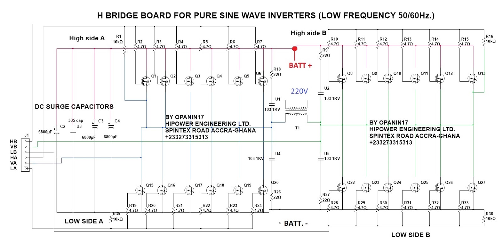
Compete circuit diagrams of h bridge are shown below.
In h bridge two mosfets are used as high side mosfets and two used as a low side mosfets. 4 transistors form the 4 vertical legs of h, and the motor is the horizontal bar in h. Dc/ac pure sine wave inverter jim doucet dan eggleston jeremy shaw mqp terms abc 20062007 advisor: Sine wave inverter circuit digram with code igbt (insulated gate bipolar transistor) module is a device required for inverter use in many types of industrial equipment, and had driven the trend
Mosfet, bjt, ijbt, or thyristor, etc.
As shown in circuit diagram, input dc voltage is vdc = 100 v. Ir2210 high and low side drivers outputs are used to drive these mosfet. Sinusoidal pulse width modulation, h bridge and low pass lc filter to make pure sine wave inverter circuit diagram. This type of inverter requires two power electronics switches (mosfet).
Tracking | this paper extends the results.
I have used ir2210 mosfet gate driver circuit. Electrical engineering questions and answers. F = 1/1.453 x rt x ct in which rt is in ohms and ct in farads.