Design & analysis of a sine wave inverter using forward converter and. As shown in circuit diagram, input dc voltage is vdc = 100 v. In half bridge inverter, peak voltage is half of the dc supply voltage.
sg3525 full bridge inverter sechmatic with pcb layout SHEMS
This circuit has no tags currently.
12+ single phase full bridge inverter circuit diagram.
A voltage source and a resistive load. Circuit diagram of single phase full bridge inverter: A power inverter, inverter or invertor is a power electronic device or circuitry that changes direct current (dc) to alternating current (ac). A full bridge topology is used to implement the dc to ac inverter.
Accordingly, it is assumed that the input dc voltage (edc) is constant and the switches are lossless.
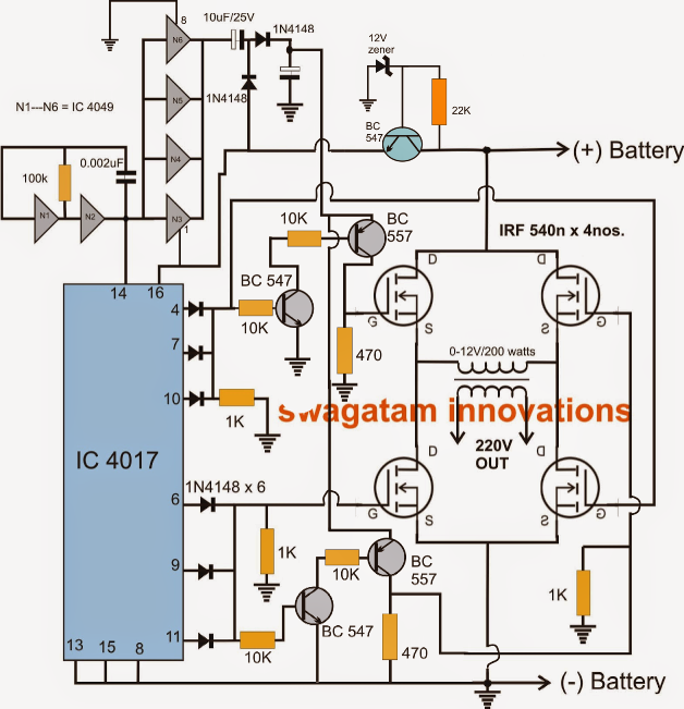
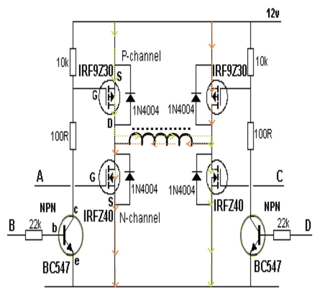
Circuit diagram of single phase full bridge inverter with r load. In full bridge topology has two such legs. Simple 150 watt full bridge inverter. The diagram above shows how to implement an effective full bridge square wave inverter design using a couple of half bridge ics ir2110.
Here the inverter circuit uses four thyristors divided into two pairs (t 1, t 2, and t 3, t 4).
The proposed arduino inverter circuit could be upgraded to any preferred higher. 1 year, 5 months ago tags. As shown in circuit diagram, input dc voltage is vdc = 100 v. Single phase full bridge inverter.
Full bridge inverter with r load :
In full bridge inverter, peak voltage is same as the dc supply voltage. This configuration consists of 2 pairs of switches that s1s2 and s3s4 which active alternately. The following image shows an example inverter circuit using the ic sg3525, you can observe that the output mosfet stage is missing in the diagram, and only the output open pinouts can be seen in the form of pin#11 and pin#14 terminations. A careful observation of the above circuit diagram reveals that power circuit of a three phase bridge inverter is equivalent to three half bridge inverters arranged side by side.
Here load is connected between two points a and b.
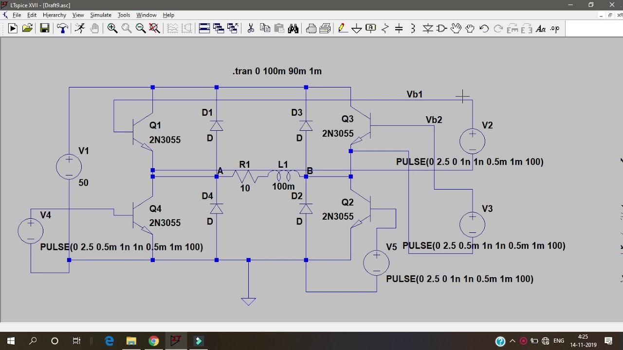
The power circuit of a single phase full bridge inverter comprises of four thyristors t1 to t4, four diodes d1 to d1 and a two wire dc input power source v s. Single phase half bridge and full bridge inverter circuit. Point a is always considered as +ve w.r.t point b. The arrangement of the inverter consists of four transistor, (mosfet or igbt).to obtain an ac waveform at the output, the transistors are turned on and off in pairs of q 1, q 2 and q 3, q 4.
1 year, 5 months ago.
200v, 3a dc power supply 20v, 100 ma dc power supply 120v/500w load bank such as resistors, light bulbs or a portable heater connection should be made according to the diagram shown on figure 1. The output current direction is considered as positive when current flow from a to b and output voltage is considered as positive when a is positive w.r.t. In a full bridge converter configuration, the dc voltage is converted to ac by switching alternatingly to reverse the polarity which connected to the load quickly. Full bridge converter is a circuit method used to convert dc voltage to ac.
If the load is purely resistive, the feedback diodes are not required.
The above topology are analyzed under the assumption of ideal circuit conditions. Each leg of the inverter consists of two series connected electronic switches shown within dotted lines in the figures. Each diode is connected in antiparallel to the thyristors viz. The main difference between half bridge and full bridge inverter is the maximum value of output voltage.
Circuit diagram of three phase bridge inverter:
1 shows single phase bridge inverter with resistive load. One pair of devices operates. Figure 3 below shows the oscillator stage of our 150 watt full bridge inverter circuit diagram and it looks pretty straightforward. Circuit diagram of single phase full bridge inverter with rl load load rl is connected between point a and b.
Multiple the project will be commenced by a basic understanding of the circuitry of the spwm inverter, the components used in its design and the reason for choosing.
4.14.if the load is purely resistive, the feedback diodes are not required. The components required for conversion are two times more than that used in single phase half bridge inverters. The circuit diagram of full bridge inverter is as shown in below figure. The use of full bridge configuration
For ideal switches the full battery voltage appears across the load.
The circuit of a full bridge inverter consists of 4 diodes and 4 controlled switches as shown below. T1 and d1 are connected in parallel, t4 and d2 are connected in parallel, t3. Sg3525 inverter circuit which can be configured with the the above discussed full bridge network. Circuit diagram of the half bridge inverter is as shown in below figure.
The integrated circuit ic1 (74hc4060) functions as a binary counter coupled with an integral oscillator.
As shown in circuit diagram, input dc voltage is vdc = 100 v. Figure below shows a simple power circuit diagram of a three phase bridge inverter using six thyristors and diodes.